Orchard Electronics Developer's Guide
Contents
Design Guide
Schematics
A page-by-page discussion of the Orchard schematics.
Overall Power Architecture
The system is designed to be powered off of a single Li-Ion cell. The primary voltage rail in the system is 3.0V, which is constrained by the nominal voltage of the NRF8001 BLE (all other components could handle a nominal voltage of 3.0V). The lower power rail is advantageous, however, as it allows us to slave an LDO directly off the Li-Ion cell and operate until the cell is basically exhausted.
The low-voltage limit of operation is actually constrained by the SSD1306 in the OLED, whose internal charge pump only operates down to 3.3V. However, best practice typically dictates not draining an Li-Ion cell to that point anyways.
VUSB at 5V is introduced to the system for charging, and also supplies the VCC of the WS2812B LEDs. When the system isn't charging, it needs a boost regulator to supply the 5V power to keep the LEDs on.
MCU
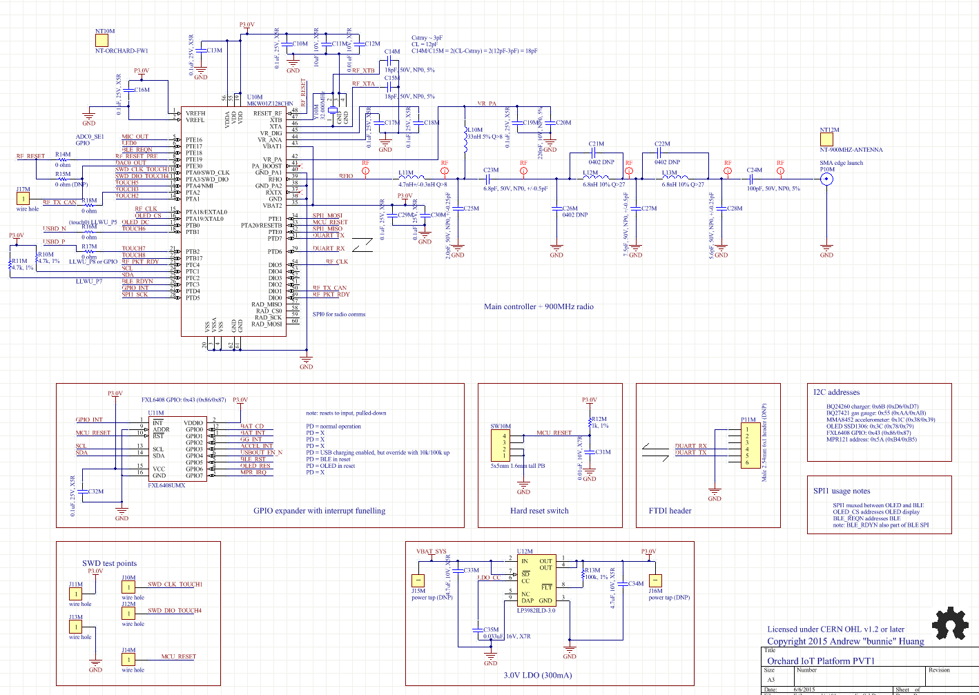
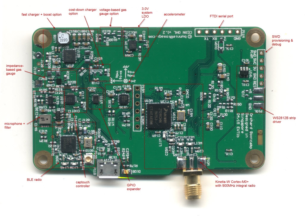
This page contains the Kinetis-W MCU, RF filter, GPIO expander, system LDO, reset switch and various test points.
CPU Design Notes The RF filter topology and component values are directly from the Freescale reference design for 900-MHz band radios. The component selection has been fine-tuned a bit to support low-cost China vendors without too much loss in performance. In lab testing, the series inductors L12M and L13M seem to be the greatest contributor to insertion loss, and thus those were upgraded to wirewound inductors from MLC inductors. We are using an SMA edge-launch connector for the antenna, but the design could also be adapted to use a microstrip, on-board cermaic, or U.FL connector depending upon the user's needs.
The accuracy of the crystal on the Kinetis-W is greatly affected by the load capacitance. On our initial prototype, we had a crystal with a CL of around 7pF, and then we switched to one with a 12pF CL without changing the parallel capacitors. That offset caused enough frequency shift to cause high bit error rates in data demodulation. So pay attention to the ppm tolerance of the crystal as well as the CL if you are re-designing that circuit.
We moved RF_RESET from its default location of PTE30 on the reference design to PTE19. The reason is that PTE30 is the one and only DAC output, and it seemed like a shame to waste it on a reset line for the radio.
Another trap on the design is that port B on the microcontroller is the only port that cannot be used to trigger interrupts. Thus, when wiring up interrupt sources to the MCU, avoid port B.
While the Kinetis MCU supports captouch on its own, we opted not to use the facility because it's poorly documented, and the scant documentation we could find indicated that the traces should be shorter than about 4-5". The problem is that we wanted to co-locate the MCU next to the RF port, which isn't always convenient for captouch surfaces. Thus to improve our chances of first-time success, we opted to use an external captouch chip with better documentation and board location.
We steered clear of using any of the DIO pins for any GPIO purposes. We opted to connect the RF packet ready and transmission FIFO not full (TX_CAN) pins, so that we could use interrupts to drive automatic FIFO filling and draining for reliable implementation of larger packet lengths without busy-waiting the CPU in a thread monitoring FIFO status.
GPIO Expander Although we could just barely cram all the signals into the MCU for the base design, as a platform we needed to have some free pins for extensibility. Thus, we included a GPIO expander. For cost-down designs that don't need to support such a rich set of peripherals, one could certainly cut the GPIO expander from the design and rework the firmware to use direct GPIO mappings.
Our choice of which pins to route to the GPIO expander was primarily static signals (reset lines, charger status lines) and less time sensitive interrupts. The GPIO expander can aggregate interrupts and fire a single pin that's then handled by firmware that queries the exact interrupt source and dispatches the correct routine based on that query.
LDO The LP3982 LDO is a reasonably inexpensive LDO (~$0.20) with very low dropout, good noise performance, and 90uA quiescent current. Cheaper LDOs can be substituted, but compared to the cost of other components in the system it seemed like a reasonable compromise between cost and performance. Also, I generally find that Nat Semi/TI regulators have better short circuit protection than the Chinese clones, and this is a desirable property for a dev platform.
The quiescent current is a bit high compared to the ultimate performance achievable by the Kinetis-W (330nA in VLLS0), but reasonable compared to Stop mode (212uA). A number of other peripherals consume current on the order of dozens of uA in standby. This metric could be improved if you're looking for extremely long battery life with the system in low power stop mode most of the time.
The LDO is slaved directly off the battery, not the boost regulator, for better efficiency. The low dropout allows for operation even when the battery is quite low.
The 300mA output of the LDO is ample for the system.
SWD The SWD pins are multiplexed with some of the touch sensor pads on the Kinetis W, which is yet another reason we opted to use an external captouch chip. The Kinetis W relies entirely upon SWD for provisioning the chip's flash memory, and thus any captouch pad design has to anticipate the need for both SWD and electrode design. We didn't like this restriction.
We add a MCU reset pad as well for SWD. It's not necessary, but it could be handy.
As an interesting side note, the Kinetis W is so "bare metal" it has no internal mask ROM firmware as far as we can tell. A factory-new device will constantly stab itself in the eye on a fault condition as it tries to execute invalid code at the reset vector. SWD is thus essential to the factory provisioning system.
USB For the purposes of charger type detection, we wire USB pins to analog inputs on the Kinetis-W. However, we also provided unpopulated board-level resistors to allow the opportunity for the Kinetis-W to respond as a low-speed USB device via bitbang protocol. The firmware isn't there to support it, but if someone writes that module the appropriate resistors are all there to allow for the device to work as a low-speed USB peripheral.
Other We provide an FTDI 3.3V compatible header for serial console support. Nominal baud rate is 115200 8-N-1. Some variants of the design include a diode on the power pin so you could in theory power the board from the FTDI cable for debugging. However, once we realized that SWD was more useful than UART, we eliminated that diode in later variants. The diode is provided because we want to avoid back-powering the USB subsystem if the board is energized from other means.
The reset switch is just a simple push button with an RC to help filter out mechanical chatter.
The page also documents all the allocated I2C addresses and SPI allocations. We encourage designers who change the design to keep this table up to date, as it's quite helpful for firmware engineers.
As an administrative note, we use the schematic symbols "NT" to indicate components that are part of the BOM but not assembled onto the board. So, for example, the firmware and the antenna (which screws into the SMA edge launch socket) are NT symbols.
Charger & Battery
There's a few architectural options. The two basic directions enabled are:
- Big, brawny, and expensive
- Small and cheap
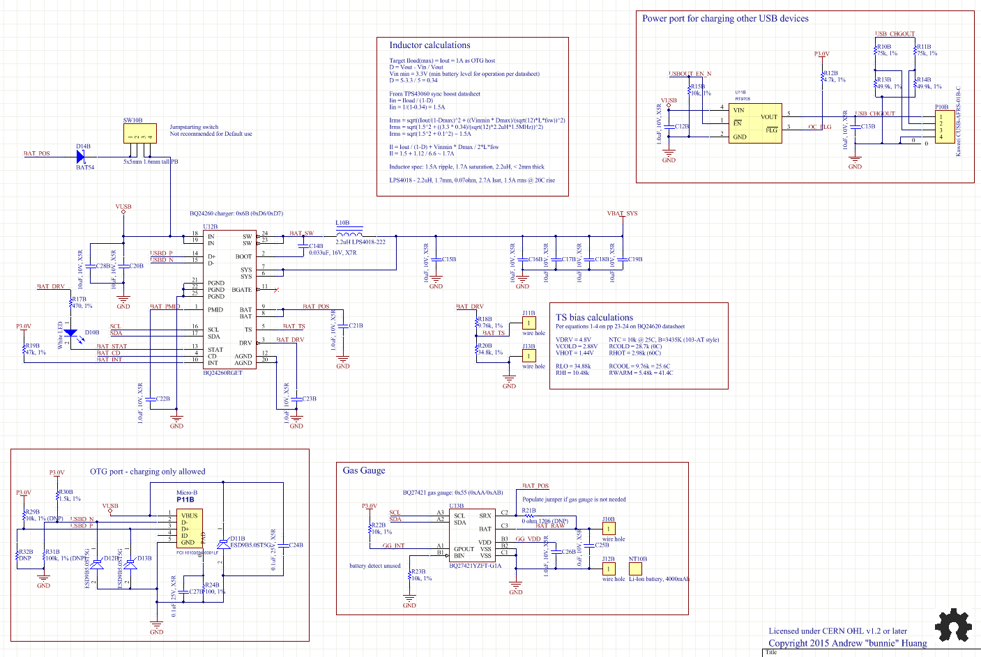
Big and Brawny For designs that need beefy batteries (>1500mAh), a BQ24260 charger is invoked. It's not cheap, but this charger can fully utilizes the current available on a CDP (at 1.5A) to charge larger batteries. It also has an integral boost regulator, so VUSB (the +5V line) can be powered up even if a charger is not present. This boost regulator is essential for driving features such as the WS2812B LED which requires a +5V source, and thus it's a nice 2-in-1 solution.
We never validated the battery temperature sensor feature on the BQ24260, as none of our batteries have an integral temperature sensor. But, the calculations are based upon a 103-AT style thermistor with a beta of 3435 kelvin and a nominal resistance of 10k at 25 degrees C.
The inductor calculations for the BQ24260 are also documented on the page. I have a preference for coilcraft inductors, and the LPS4018 is a nice low profile solution with high saturation current for its size.
I opted to use multiple parallel filter caps on VBAT_SYS instead of a single larger one to reduce ESR and also simplify the BOM. Since this design is intended for smaller runs, quadrupling-down on 10uF capacitors means you burn through a reel of the parts faster. Using a 47uF cap would be both more expensive and also more parts wasted at the end of a short run. However, if board space is a premium, then condensing C16B-C19B into a single part is warranted.
We felt that the internal conduction loss of the system transistor for the BQ24260 is adequate, and thus we don't use an external transistor via BGATE.
BQ24260 is a variant of the regulator that features automatic D+/D- recognition. In practice, we found that the feature works so-so, especially if you're relying upon the system to boost voltage; for unknown reasons the charger capacity identification would tend to fail. Instead, we mapped microcontroller pins to D+/D- and do charger detection that way and override the BQ24260's readings.
One neat feature of the BQ24260 is it also supports auto charge rate reduction if the input voltage is seen to be drooping.
Another convenient feature of the BQ24260 is that it has a built-in "shipping mode" where the battery is fully isolated from the system, allowing you to safely ship a device with the battery installed. Getting out of "shipping mode" requires you to plug in USB power.
All of these features come at a small burden on the firmware, i.e., the chip needs a bit of configuration, and it also requires to be constantly pinged by a watchdog while in boost or in charging mode. The requisite firmware to do this is fairly complete.
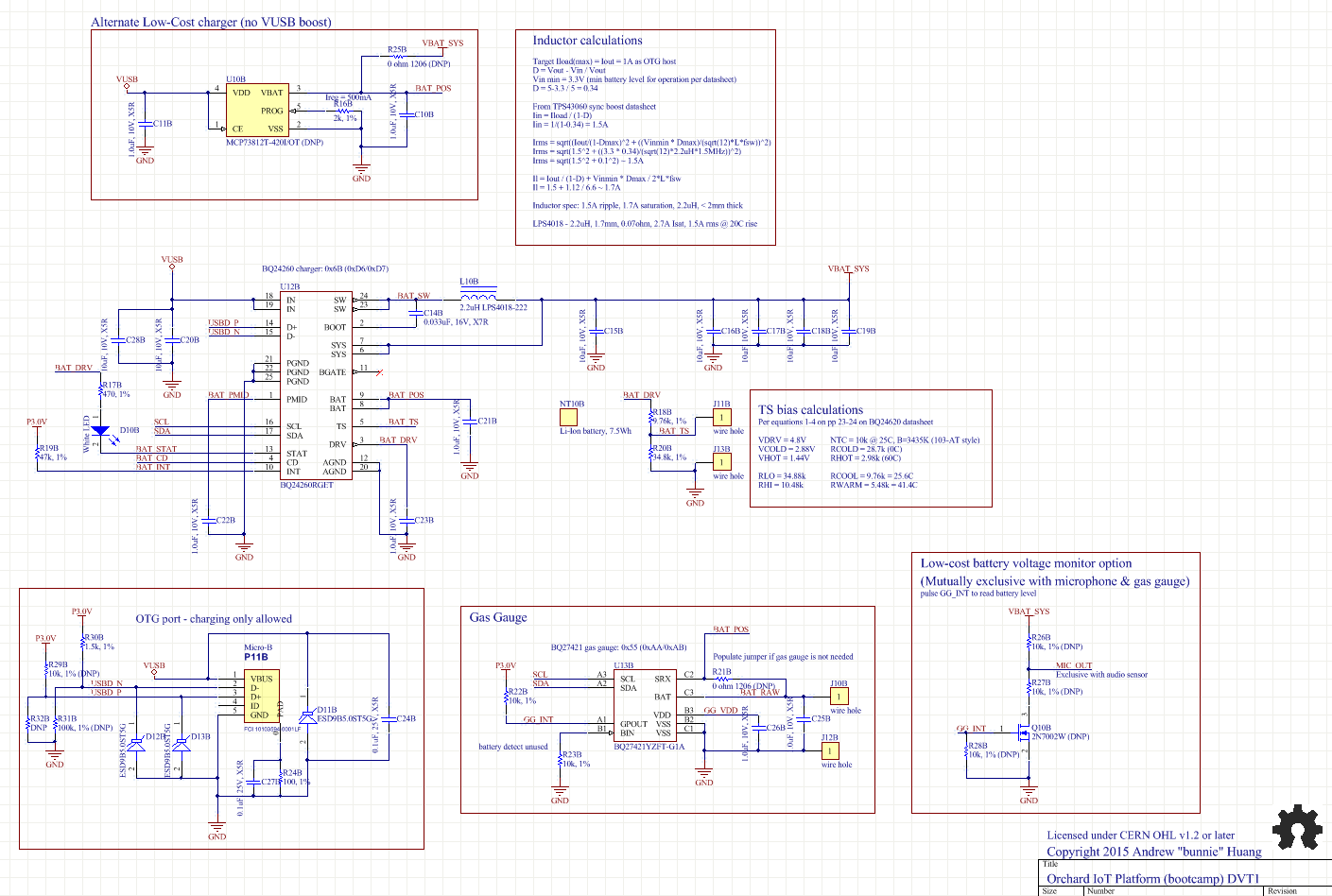
Small and cheap On some variants of the design, pads are provided to alternately populate an MCP73812T. Note that we never validated this circuit, but it's there in case someone wants to try it. This is a cheap, single-chip linear regulator charging solution set to 500mA with a resistor. According to the datasheet, it pretty much just "does the right thing" without any firmware programming.
Downsides:
- no boost regulator -- so you lose the ability to have a +5V line on the system that's active on battery
- no "shipping mode" switch, which may be critical for applications where you need to apply for an air shipping license without a removeable battery
Gas Gauge options We provide two gas gauge options: impedance tracking, and voltage tracking.
Impedance tracking is expensive -- about $1-$1.50 in quantity, and twice that in distribution -- but can provide a very accurate sense of remaining battery life. It also provides real-time status on current draw. As a development tool, it's well worth the money. The tiny BGA CSP package can be annoying to hand-assemble, but most technicians in China are fine with it. It's also designed for system-side use, e.g. with a replaceable/swappable battery.
For designs that can't afford such a deluxe battery status tracker, some designs implement an NFET switching out a voltage divider on VBAT_SYS feeding into an ADC on the MCU. Straight up voltage readings are a poor predictor of battery level; you need to go through a translation function that turns the voltage into a capacity figure, and that depends upon the loading of the system versus the battery's impedance.
However, the provision of both impedance tracking and voltage tracking does allow for the possibility of writing firmware that automatically extracts a table of voltages corresponding to remaining capacity using the impedance tracker state of charge metric plus simultaneously sampled voltages using the ADC (you couldn't use GG_INT but you wouldn't need it for this application). This curve would be fairly consistent within a particular type of battery made by a particular vendor and could be fairly reliable. However, any change in battery vendor or capacity would require a recalibration. Also, the calibration would depend upon the current draw, so the reading would have to assume that the system is drawing either much less than C for the battery, or its current consumption characteristic is fairly uniform across the entire operating regime.
Note that the impedance tracking gas gauge draws about 93uA in normal mode, but will automatically sleep/hibernate to reduce current to between 9-21uA. Since it's on the battery side of the isolation switch in the charger, this drain is always present on the battery and should be factored in when calculating battery shipping lifetimes. The "big" charger itself draws around 15uA max in shipping mode.
MicroUSB OTG port The OTG port is a bit over-designed. I decided to include full ESD protection, in case one was trying to apply for CE immunity testing where they zap all surfaces with 8kV. The metal case of the micro-USB connector is coupled to ground via an RC, which means it's a terrible ground test point but also ESD won't couple into the ground plane causing the system to upset during immunity testing.
Power port The boost regulator on the BQ24260 can source up to 1A, which means there's some headroom to allow orchard to serve as a dumb battery pack to charge other devices. For some high-capacity configurations and user scenarios, being able to use the system as a battery charger in a pinch is pretty handy, and the cost of adding the feature is minimal.
An RT9706 current limit is provided to prevent over 0.5A from going out the USB port, leaving another 0.5A of the 1A boost capacity for internal system use. A resistor network, snagged from the Adafruit Mintyboost 3.0 design, is provided across D+/D- that according to her documentation, generally fools most smartphones into believing there's a non-trivial power source on the other side. This hasn't been rigorously tested.
Sensors
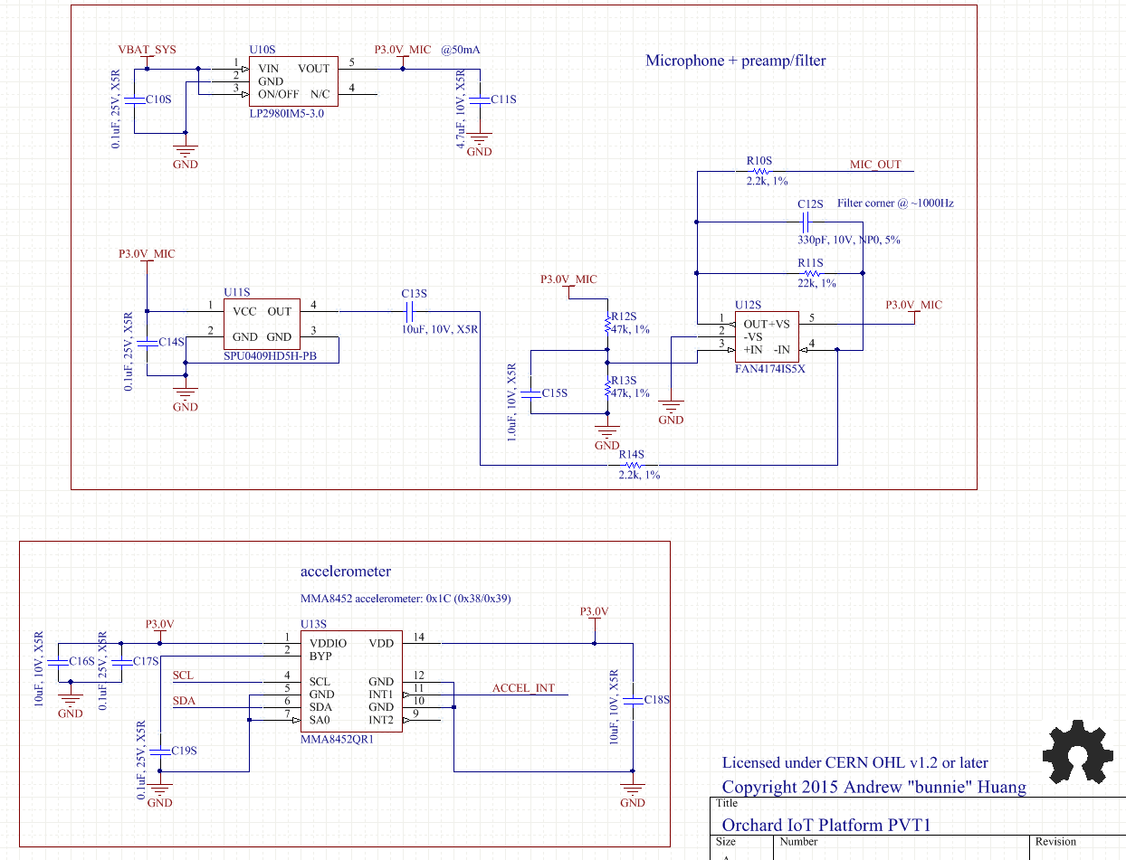
This page contains a microphone and accelerometer sensor.
We recommend most new sensors added to be direct-digital sensors, e.g. have I2C outputs to avoid iteration around analog design, particularly if the designer is a novice.
The accelerometer is an example of a gravity-to-digital sensor. It's a 3-axis accelerometer accelerometer, the MMA8452, and it's sold in massive quantities at a decent cost. One of the interrupt lines is wired to the CPU to allow for efficient free-fall or hit detection. It's good a good dynamic range, and offers sampling rates up to 800Hz.
The microphone + pre-amp is a tried-and-true design adjusted from the Chibitronics sound sensor sticker. A silicon microphone is used for ease of process integration (no pigtails or wires to solder). The microphone feeds via a DC blocking cap into a rail-to-rail op amp, the FAN4174. It's one of my favorites; versatile, cheap, and good performance specs overall. R12S and R13S form a bias network that centers up the microphone signal at 1.5V, the mid-zone of the ADC; C15S helps improve performance against power supply noise.
The gain is set fairly low, at 20dB. The microphone has a sensitivity of -42dB/Pa, so the net system has a -22dBV/Pa gain which means a swing of 0.22V at 94dB sound pressure. This is about right for continuous operation in a club or concert environment, where SPL is around 100-105dB giving us about a 1Vp-p swing. If we wanted to be more sensitive on the quiet end, the gain could be bumped up by about 5x or 10x.
C12S adds a filter corner of around 1kHz on the signal. The filter corner can be adjusted per application but the target of this particular schematic is picking up bass in a concert environment.
R10S is not strictly necessary but it helps reduce capacitive loading on the FAN4174, improving stability.
U10S is an LP2980, which is an LDO for the microphone circuit. Because we're generating a reference voltage by dividing down the power supply via a resistor, our noise rejection on the power supply is pretty poor. Unfortunately, most techniques I could use to generate the bias would involve active components around the same cost as an LDO, so I figure why not bite the bullet and just use a regulator that isolates the whole microphone circuit from all the switching noise on the rest of the design. In particular, a board with radio PAs bursting packets and WS2812's PWM'ing away will create a heck of a lot of power supply noise and the local LDO just makes all of that go away. Probably a cheaper, more modern LDO could be used in the place of the LP2980, this is a part I've been using for years and could use a refresh.
The mic circuit draws about 80uA (LP2980) + 145uA (microphone) + 200uA (amplifier), so it's a pretty big current draw (425uA) during sleep modes. If very low power sleep is needed, wire up the on/off from the LP2980 to a GPIO on the MCU, this will drop current to < 1uA.
For reference, the accelerometer standby current is 1.8uA.
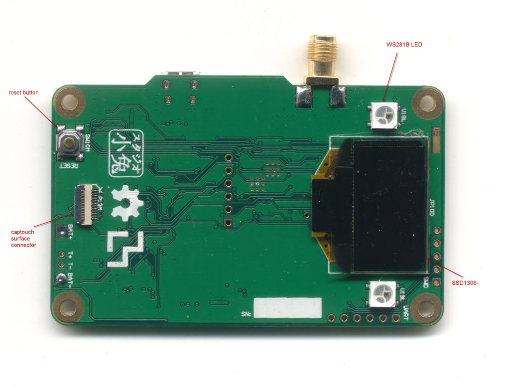
OLED
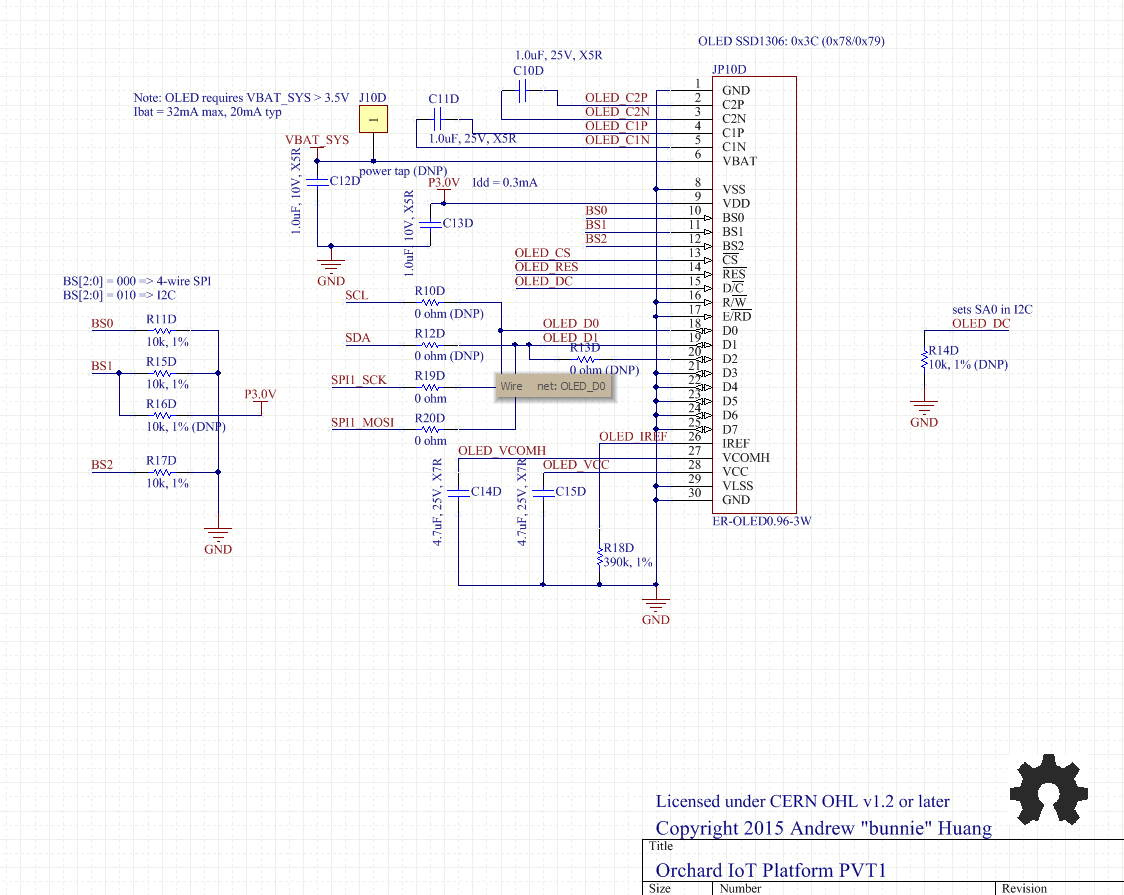
We use an OLED with a Solomon Systech SSD1306 controller. The display itself is sourced from East Rising, and for cost reasons it's a small, 0.96" black and white display. Certainly, a user could use a more fancy full-color OLED if their application demands it.
We use the OLED display in its self-biasing mode, which saves some component count on bias generation. Again, as much as possible we try to slave regulators directly off the battery for better efficiency. Overall there isn't too much ripple on the display, although we do see a tiny bit of brightness droop with certain patterns on the screen. The good news is that the charge pump topology is inductor-free, so there's no potential for audible noise from inductor windings. For some reason, maybe it has to do with the refresh characteristic of the OLED, I tend to get a bit of a whine out of the inductors in boost regulators that feed OLED displays.
C10D, C11D, C14D and C15D are all rated to 25V. This is much higher than the OLED voltage spec but ceramics tend to derate at higher voltages, and the performance of these capacitors will be critical for good image fidelity.
The OLED has two wiring options built into the PCB: one via I2C, and the other via SPI. For production, we use SPI as it's faster, but there are scenarios where I2C could be appropriate (for example, if users are at a hard pin count limit on the MCU and can't afford the extra wires for the SPI). Both interfaces have been validated and shown to work.
BLE
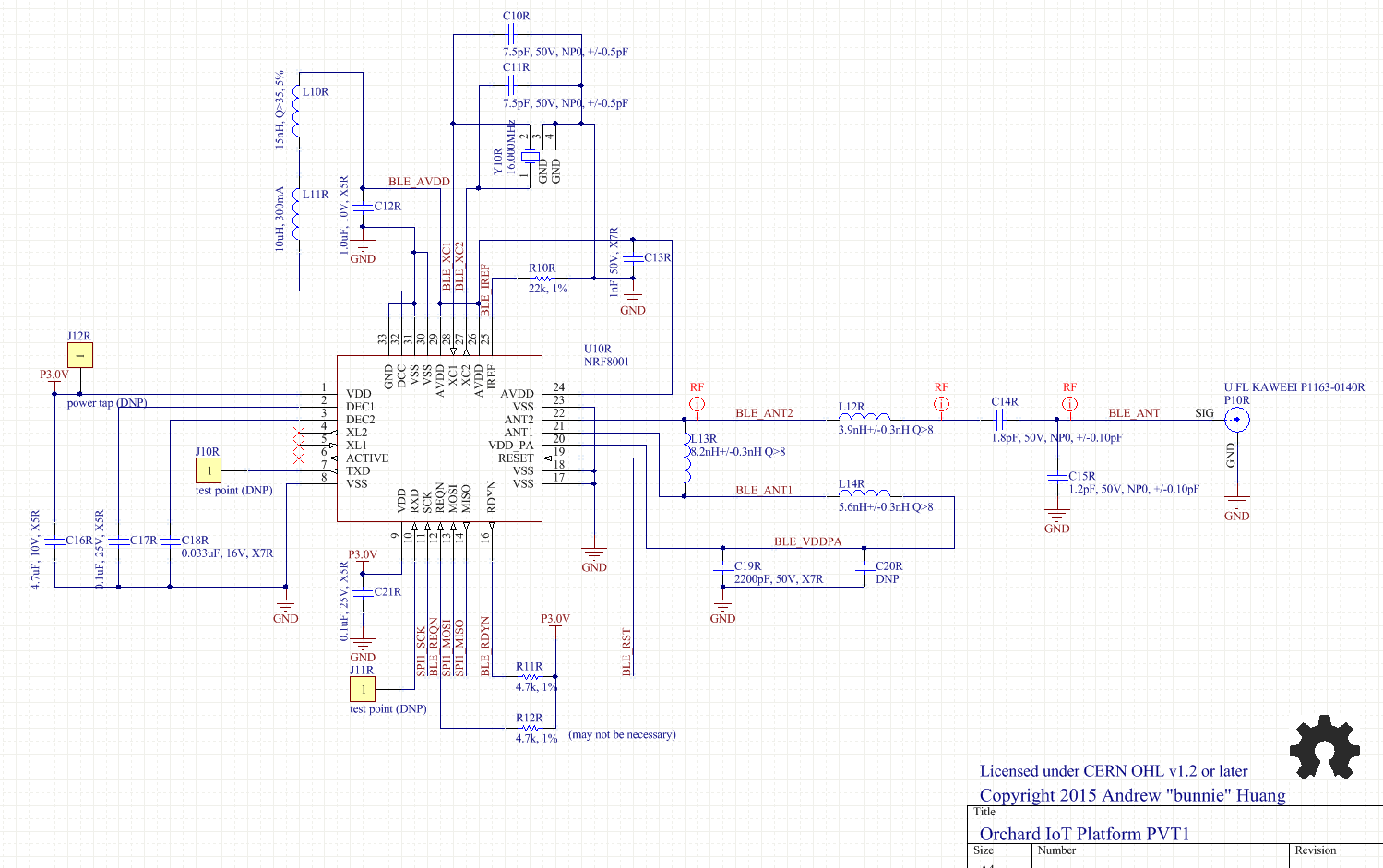
The BLE design is essentially a straight copy of the Nordic reference schematics. There's not much to the design, anyways.
Deviations of note are that CL on the crystal (C10R and C11R) have to be adjusted to 12pF to match the production crystal CL of 9pF.
The design topology used here invokes the switching regulator for the PA. It seems the firmware currently doesn't activate the switching regulator, yet we still see a solid 3.0V on AVDD. Not sure if this is because the switching regulator automatically bypasses when the voltage is low enough.
The inductor types were optimized for low cost and ease of sourcing in China.
The antenna port is currently a U.FL connector, but can be replaced with microstrip, ceramic, SMA, etc. as needed by the final design. I prefer to use U.FL connected antennae as it simplifies mechanical integration -- you often times want the antenna at a place that's really inconvenient for a microstrip implementation, but for cost and compactness a microstrip could be better.
LED
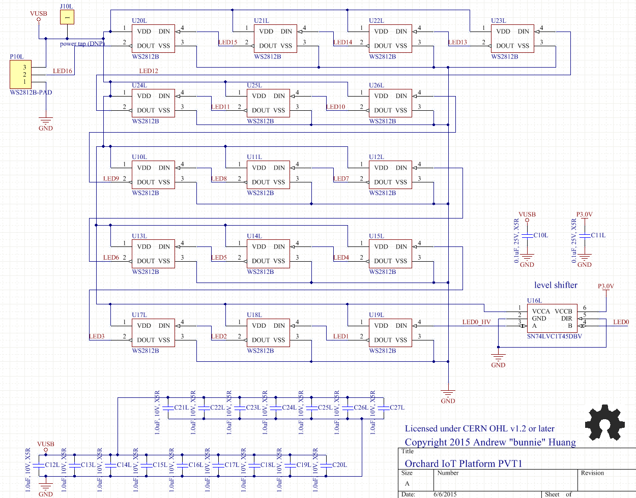
This is the LED array provided for the burning man edition of the Orchard design. As it's burning man, lots of LEDs are desirable. For the bootcamp reference, we only use two LEDs simply to demonstrate the functional possibility of including them.
A level shifter (74LVC1T45DBV, U16L) is necessary as the LEDs require 5V CMOS signals, but the MCU only outputs 3.0V CMOS.
The WS2812Bs have ample decoupling with 1uF per LED. They are noisy and chop the power supply a lot since they are PWM'ing 3xLEDs that can draw 20mA each.
A footprint for soldering on a longer LED strip is provided, in case you want more LEDs than provided in this design.
Captouch
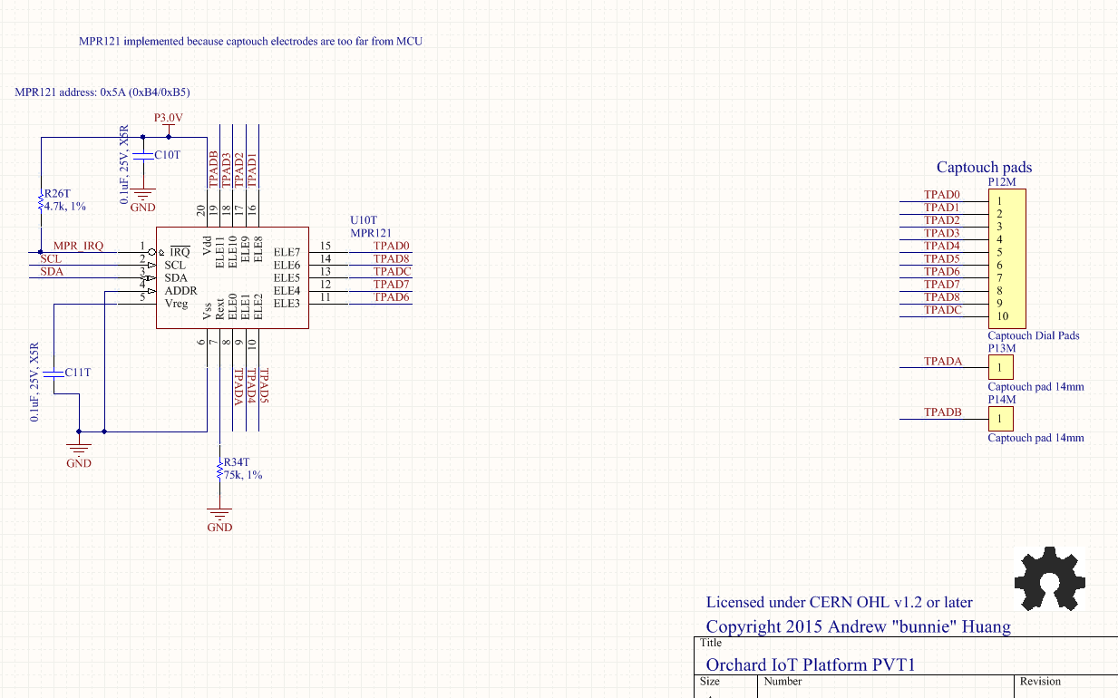
The MPR121 captouch controller is provided because the electrodes for touch are too far away from the MCU for reliable implementation. While it may be possible to use the controller in the MCU, ferreting out all the interference problems would probably take a couple board spins. Designs going to volume production may find it worthwhile to iterate to eliminate the cost of the MPR121, however, the MPR121 has proven to be a fairly robust controller once its firmware is set up correctly. It turns out that the reference code from Sparkfun is bunk and the cal values they pick for defaults are terrible; it takes several minutes for electrodes to equalize and they don't work well for electrodes covered by a bezel. The Orchard firmware picks cal values that find home a bit quicker, and also includes a fast-cal step on boot to equalize baseline values quickly.
MPR121 integration on the burning man edition drives a captouch surface fabricated directly onto the PCB, for lower cost.
MPR121 integration on the bootcamp uses a custom flex PC bonded to a plastic case for better appearance.
The MPR121 shutdown current is 3uA, hence no load switch is provided for it.
High-Res Photo Guide