GPBB User Guide
The GPBB is a good entry point for most hardware hacking applications on Novena. This document describes in some detail about the function and theory of operation behind the GPBB.
Contents
GPBB Features
- Digital I/O
- 16 digital outputs organized in two 8-bit banks (A and B)
- Each bank can be individually tri-stated
- 8 digital inputs organized in a single 8-bit bank
- Switchable I/O voltage
- I/O VDD software switchable between +5V and a lower voltage
- Lower voltage I/O VDD nominally set to 3.3V but adjustable changing out a single resistor
- I/O VDD current-limited to 500mA
- In 5V mode, overcurrent indicator available
- I/O VDD can be sampled by on-board ADC to verify operation
- LEDs
- Four green LEDs
- Connected to port B bits 0-3
- Analog Input
- 6x 10-bit analog inputs
- 0-4.7V full scale range
- AVDD set by local LDO to +/- 1.5% accuracy
- Up to 200 ksps conversion rate
- Upgradable to 12-bit accuracy by swapping out ADC chip
- DAC-to-ADC loopback and VDD/IO measurement paths available
- Analog output
- 2x 10-bit analog outputs
- 0-3.3V full scale range
- Output speed limited by I2C bus rate (100kHz I2C -> ~5kHz output rate)
- Upgradable to 12-bit accuracy by swapping out DAC chips
GPBB Host Interface Features
The host interface to the GPBB is implemented using the FPGA. It is configurable, and therefore, this feature list should not be considered etched in stone. There is a lot of flexibility on how to implement the host interface, and this particular configuration was chosen to maximize the pedagogical value of the GPBB reference design.
- EIM register interface
- Modular, scalable register interface
- FPGA version reporting
- Loopback testing
- Control of the digital input and output ports
- CPU-> FPGA I2C register interface
- Example of communicating with the FPGA via I2C
- Control and readout of the ADC
- FPGA version reporting
- Loopback testing
- CPU->DAC I2C interface
- Direct bus interface to I2C with expansion card components
- Example of using expansion port with no FPGA intervention
- 2x DAC chips connected to CPU I2C bus (DACA is at 0x14, DACB is at 0x12)
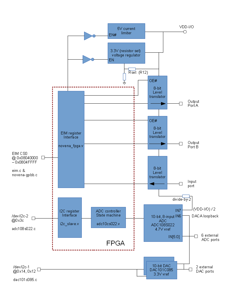
Block Diagram
This is a simplified block diagram of the GPBB. Consult the schematic for more details.
Some blocks/IOs are annotated with filenames strongly associated with those features, in case you want to skip reading the documentation and just go for the source.
Hardware Photo
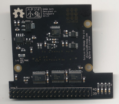
Note R12, the voltage set resistor, is in the mid-left of the board in this photo.
Setting the I/O Voltage
The low voltage setting for the I/O is defaulted to 3.3V.
You can change this by desoldering R12, the larger 1206 resistor, and replacing it with one of the following:
- 316 ohm for 3.3V (default)
- 215 ohm for 2.5V
- 124 ohm for 1.8V
If you don't want to desolder the 316 ohm resistor, you can:
- Parallel a 680 ohm resistor with the default 316 ohm resistor to get 215 ohms
- Parallel a 200 ohm resistor with the default 316 ohm resistor to get 122 ohms
The 1206 resistor is large enough so one can fairly easily parallel an axial resistor across the surface-mount device.
Command-line Firmware Example
A command-line example program of using the GPBB can be found on github at
https://github.com/bunnie/novena-gpbb-example
Before running the example program, you must configure the FPGA. You can do so using the shell script included in the above git repo as follows:
sudo ./configure.sh novena_fpga.bit
The shell script basically configures the FPGA configuration reset pin, flips it (so the FPGA is erased), and then dd's the bitfile to /dev/spidev2.0.
The example program must be run as sudo, as it uses the /dev/mem interface to access the memory-mapped EIM CS0 and CS1 regions.
The built-in help describes the usage of the program:
bunnie@bunnie-novena-laptop:~/code/novena-gpbb-example$ sudo ./novena-gpbb
Usage:
./novena-gpbb [-h]
        -h  This help message
        -v  Read out the version code of the FPGA
        -da <value> set DAC A to value (0-1024 decimal)
        -db <value> set DAC B to value (0-1024 decimal)
        -a  <chan> set and read channel <chan> from ADC
        -hv set VDD-IO to high (5V) voltage
        -lv set VDD-IO to low (nom 3.3V unless you trimmed it) voltage
        * GPBB has two 8-bit output-only ports (A,B), and one 8-bit input port
        -oea <value> drive I/O bank A (value = 1 means drive, 0 means tristate)
        -oeb <value> drive I/O bank B (value = 1 means drive, 0 means tristate)
        -p <port> return last written <port> value in hex, port is [a,b] (note these ports are output-only)
        -p <port> <hex value> set <port> to <hex value>
        -p_set <port> <bit>  set <port> <bit>
        -p_clr <port> <bit>  clear <port> <bit>
        -rp return the value of the 8-bit input port
        * CS1 isn't useful in the design, but loopback code provided as a template
        -testcs1 Check that burst-access area (CS1) works
The test program incorporates all three interfaces (EIM CS0, I2C-1, and I2C-2) to drive the various interfaces. It also has an EIM CS1 example to mirror the example of using the burst-mode CS1 interface.
Burst-mode EIM access is provided for applications that require a high bus utilization. The i.MX6 takes about 32 cycles to turn the bus around between burst memory operations to the region. Thus, the CS0 interface, which transfers only one 16-bit word at a time, can achieve only about 3% utilization of the bus. Burst mode will perform a 64-bit access (4 words in an access) trivially, and can extend to much longer bursts with properly coded FPGA hardware. Even using the 64-bit accesses triples utilization to 10%. The example implemented in this codebase just does a loopback write/read of the CS1 space.
File structure
Code to read the adc is in adc108s022.c. In particular, look at adc_chan() and adc_read()
Code to write the dac is in dac101c085.c. In particular, look at dac_a_set().
Code to modify the digital I/O ports is in novena-gpbb.c. In particular, look at gpbb_write_port() and gpbb_read().
The dirty and mind-bending details of setting up CS space in EIM can be found in setup_fpga() and setup_fpga_cs1(). The i.MX6 docs are really bad on EIM, so many parameters were verified using an oscilloscope to disambiguate the rather poor documentation. If you want to muck with these, make sure you have an oscilloscope or a ChipScope JTAG logic analyzer for the FPGA to validate your understanding.
Kernel memory access is done using write_kernel_memory() and read_kernel_memory().
Note: failing to call setup_fpga() or setup_fpga_cs1() before accessing EIM via these calls will cause your Novena to hard-lock.
eim.c and eim.h are vestiges of an attempt to modularize the EIM code, but never finished.
FPGA Details
The FPGA implementation can be found at
https://github.com/bunnie/novena-gpbb-fpga
The design is targeted to a Xilinx Webpack ISE "PlanAhead" flow (downloadable for free (but not open source) to run on x86 machines), so the novena-gpbb.ppr file would be the project container. This code is tested against Webpack ISE version 14.5 and can achieve 100% timing closure.
Project Structure
For those who have never used a Xilinx FPGA project before, there are a few things to be aware of.
- There is a constraints file (I refer to it as a ".UCF"), novena.ucf, that maps logical top-level ports to physical pins, and also sets timing parameters to guide the place & route engine.
- Xilinx features "IP" blocks that are defined using XML (such as bclk_dll.xci and synthesized using their CORE Generator tool. This design features three IP blocks, all of them for clock and timing management.
- The directory structure of the github repo matches the default structure that the Xilinx PlanAhead tool generates.
- There is a top-level PlanAhead project descriptor file called novena-gpbb.ppr.
Code Architecture
There is a top-level file, novena_fpga.v, which contains the following:
- FPGA logical I/O definition (in the module header)
- Instantiation of the ADC state machine
- EIM register set implementation
- I2C module
- Master reset synchronizer
- Three DLLs for clock skew management
- Manually instantiated I/O primitives
- The "heartbeat" LED counter
EIM registers
EIM registers are integrated in the top-level block, instead of sequestered into a module, because typically EIM registers are used at the top-level to control sub-module controls. The trade-off is the top-level module is a bit cluttered at the convenience of being able to whack in a new register with a few lines of code.
CS0 registers
The key code templates you need to know are these:
   reg_wo reg_wo_40000 ( .clk(bclk_dll), .bus_a(bus_addr_r), .my_a(19'h40000),
			 .bus_d(din_r), .we(!cs0_r && !rw_r), .re(!cs0_r && rw_r), .rbk_d(ro_d),
			 .reg_d( r40000wo[15:0] ) );

   reg_ro reg_ro_41000 ( .clk(bclk_dll), .bus_a(bus_addr_r), .my_a(19'h41000),
			 .bus_d(ro_d), .re(!cs0_r && rw_r),
			 .reg_d( r40000wo[15:0] ) );
The module "reg_wo" implements an EIM write-only register, e.g. an output from the CPU to the FPGA fabric. The argument ".my_a" tells the module instantiation what address it goes to, in this case 0x40000. The argument ".reg_d" says what logical 16-bit net to assign to that register's state variable.
The module "reg_ro" implements an EIM read-only register, e.g. an input from the FPGA fabric. The argument ".my_a" tells the module instantiation what address it goes to, in this case 0x41000. The argument ".reg_d" says what 16-bit logical net forms the input from the FPGA fabric.
In this simple example, we loop the output of the reg_wo instance reg_wo_40000 to the reg_ro instance reg_ro_41000 using a logical 16-bit net r40000wo[15:0].
If you want to add another register:
- Copy the respective reg_ro/reg_wo template line
- Change the instance name so you have a unique instance identifier, e.g. reg_wo_40002
- Update the .my_a to the address you want the register to be at, e.g. .my_a(19'h40002)
- Update the .reg_d to your logical net, e.g. .reg_d( my_control_net[15:0] )
CS1 registers
CS1 registers are similar to CS0 registers, but they are mapped to a different chip-select bank. Each chip select bank in the i.MX6 can have different timing characteristics assigned to them, and CS1 is optimized for burst access for higher throughput. The instantiation templates here look like this:
    reg_wo_4burst reg_wo_4b_C04_0100( .clk(bclk_dll), .bus_ad(eim_din), .my_a(19'h4_0100),
				     .bus_a(EIM_A[18:16]), .adv(!EIM_LBA), .rw(EIM_RW), .cs(!EIM_CS[1]),
				     .reg_d( burst_ctl[63:0] ), .rbk_d(ro_d_b), .strobe(burst_stb) );

   reg_ro_4burst reg_ro_4b_C04_1000( .clk(bclk_dll), .bus_ad(eim_din), .my_a(19'h4_1000),
				     .bus_a(EIM_A[18:16]), .adv(!EIM_LBA), .rw(EIM_RW), .cs(!EIM_CS[1]),
				     .reg_d( rC04_0000wo[63:0] ), .rbk_d(ro_d_b), .strobe(burst_rbk_stb) );
The usage is almost identical to CS0 except that instead of a 16-bit internal bus width, the burst registers are fixed at 64 bits (and thus the addresses should go up by 8 bytes, and not 2 bytes, when assigning them). Furthermore, these primitives incorporate the concept of a .strobe() output. The .strobe() output pulses for one clock cycle after the register has been accessed or updated. This is useful if you want to sequential writes to a FIFO, for example, without having to ping-pong between a control update bit and the data itself.
If you don't need the strobe, you can simply delete it from the port argument list and the compiler will optimize the hardware out for you.
I2C registers
Unlike the EIM, I2C registers are entirely contained within a sub-module. This mean adding and subtracting I2C registers requires a little more work, but it's cleaner for code readability.
The i2c_slave module has a set of arguments, named by convention .reg_##(), which map to internal I2C registers:
   i2c_slave i2c_slave(
		       .SCL(I2C3_SCL),
		       .SDA(SDA_int),
		       .SDA_pd(SDA_pd),
		       .clk(clk25), // nominally 26 MHz, this is close enough
		       .glbl_reset(reset),
		       .i2c_device_addr(8'h3C),

		       // outputs from I2C block (CPU->FPGA) 0-3F
		       .reg_0(reg_0_test),

		       .reg_2({adc_go,adc_chan[2:0]}),
    ... );
By convention I map I2C registers 00-3F as outputs (e.g. write-only) and 40-7F as inputs (e.g. read-only). You don't have to obey this convention.
To add an I2C register, you will need to open i2c_slave.v, and add ports to the module definition:
		  output wire [7:0] reg_0,  // 00-3F are write-only (from the host perspective)
		  output wire [7:0] reg_2,
                  output wire [7:0] reg_3,  // added for this example

		  input wire [7:0]  reg_40, // 40-7F are read-only (from the host perspective)
		  input wire [7:0]  reg_41,
                  input wire [7:0]  reg_43, // added for this example
Around line 451 you'll find the area where the I2C register mappings then happen:
   assign reg_0 = I2C_regblock[6'h0];
   assign reg_2 = I2C_regblock[6'h2];
   assign reg_3 = I2C_regblock[6'h3];  // 0x3 write-only added for this example

   always @(*) begin
      case (I2C_addr[7:0])
	8'h40: begin
	   I2C_regread_async = reg_40;
	end

	8'h41: begin
	   I2C_regread_async = reg_41;
	end

	8'h43: begin                   // 0x43 case added
	   I2C_regread_async = reg_43; // 0x43 read-only added
	end
Then you'll need to save this file, go back to novena_fpga.v, modify the i2c_slave instantiation to add the .reg_3() and .reg_43() ports, and then assign logical nets from there.
Pin mapping convention and UCF tour
By convention I use the PCB schematic names as much as possible for the FPGA top-level logical I/O definition, so you don't need to go into the .UCF to figure out what PCB trace goes to what inside. Then, I use a set of assign statements to map the physical I/Os to internal meanings. So, for example, you'll see
output wire F_LVDS_P11,
output wire F_LVDS_N11,
output wire F_DX,
etc. If you look at the schematic, you'll see these are names used on the expansion header that corresponds to very specific pin mappings. These are mapped to a "meaning" later on using
  assign F_LVDS_P11 = cpu_to_dutB[0];   // LED 0
  assign F_LVDS_N11 = cpu_to_dutB[1];   // LED 1
  assign F_DX1 = cpu_to_dutB[2];        // LED 2
The FPGA top-level logical I/O definitions are mapped to physical FPGA pins in the .UCF file, e.g.:
NET "F_LVDS_N11" LOC = T11;
NET "F_LVDS_N11" IOSTANDARD = LVCMOS33;
NET "F_LVDS_N11" SLEW = SLOW;
NET "F_LVDS_P11" LOC = R11;
NET "F_LVDS_P11" IOSTANDARD = LVCMOS33;
NET "F_LVDS_P11" SLEW = SLOW;
As you can see, in the .UCF logical names (F_LVDS_N11) get mapped to a package pin (T11), a well as assigned attributes such as the logic standard (LVCMOS33) and electrical properties (SLEW = SLOW). Other things like pull-ups, termination resistors and so forth can be added at this point. The most difficult bugs are often attributable to errors in the .UCF file, so don't forget that this file exists. To be clear, here are some headaches that happen with a wrong .UCF:
- Top-level FPGA logical pins that aren't in the .UCF (e.g. due to a typo) will be mapped by default to a random pin on the FPGA. This is no good.
- The slew rate spec of a pin can have a big impact on timing closure. However, you don't want to make all pins fast because there is a limit on how many fast-slew pins you can have that switch simultaneously (it's surprisingly low, search for SSO in this document for details on why).
.UCF also contains timing closure annotations, and placement directives, such as:
OFFSET = IN 4125 ps VALID 4750 ps BEFORE "bclk";
OFFSET = OUT 5100 ps AFTER "bclk";
The above sets the setup/hold time requirement for the EIM bus
NET "reg_wo_40010/state[*]" TIG;
NET "reg_wo_41012/state[*]" TIG;
The above tells the timing-driven place and route engine to ignore these register bits during timing closure, as they are driving asynchronous destinations. Relaxing which paths the place and route engine have to pay attention to helps your design compile faster and achieve better results on the paths that do matter.
INST "oddr2_eim0" IOB =FORCE;
INST "oddr2_eim1" IOB =FORCE;
The above tells the mapper to force primitives named oddr2_eim0 and oddr2_eim1 into the IOB (actually, now that I think of it, the ODDR prims probably go to an IOB by default but I introduced this constraint to make sure it's not optimized out by some other setting).
NET "bclk" TNM_NET = "bclk_tnm";
TIMESPEC TS_bclk = PERIOD "bclk_tnm" 133 MHz;
The above defines a "timing net" and assigns a clock period timespec to it, which tells the timing-driven place and route engine what speed it needs to achieve on your design to run at the EIM speed, e.g., 133MHz. Without this, it will just do whatever and compute for you the speed it achieved, which is often times lower than what you require for correct operation.
Versioning Convention
By convention, I report the FPGA version on both the I2C and the EIM interfaces. Of course, this introduces the possibility that the version is out of sync if you forget to update in both places, and this could be address by using a parameter directive in the verilog.
However, the key point is you'll want version info on at least one interface, and it's a good way to check and see if the system is functioning correctly (e.g. all drivers loaded correctly, FPGA configured, etc.) and that you're actually using the most recent bitfile (you'll be surprised how many "bugs" happen because people forget to copy the compiled bitfile out from the Xilinx directory and re-program the FPGA with it).
Version numbers are kept at I2C register offsets 0xFC-0xFF, and EIM offsets 0x41FFC and 0x41FFE:
- EIM 0x41FFC / I2C 0xFC-FD is the minor version code
- EIM 0x41FFE / I2C 0xFE-FF is the major version code
The minor version code is used to track the version of the current project you're working on.
The major version code is used to distinguish between projects. There isn't a convention yet to distinguish or manage major version codes, but for example, it's important to distinguish between the FPGA design for the GPBB (major version 0xB) from the FPGA design for the oscilloscope (major version 0x3) or the FPGA design for SD card hacking (major version 0x1).
- For starters, kosagi is consuming major version codes where the MSB are 0x00 (so versions 0x0000-0x00FF are for kosagi).
- One-off designs are being assigned version codes where the MSB is 0xF0. If you get a version number with 0xF001, for example, you'll want to question where it came from as it may not be compatible with your hardware.
Further Reading
FPGA Hacking in the Novena Guide gives some examples how to use the GPBB