FPGA getting started
Contents
Hello World with FPGA on the Novena Board
Introduction
The FPGA is an interesting part of the Novena board but it needs some effort to get started. I just started development on the FPGA myself so I hope I still remember most of the pitfalls ;)
The FPGA can be seen as a lot of logic blocks (AND/OR/..-gates and flipflops for example) that can be interconnect at runtime. There are higher level languages to describe how you want those connections to happen called "Hardware Description Languages" the two most common ones are Verilog and VHDL. We will use VHDL in this tutorial since I'm a bit more fammiliar with it.
For the Spartan6 FPGA on the Novena we will use the ISE Design Suite and install the WebPACK edition. There are some documents on the Internet on how to install ISE.
Project Setup
Now that you have installed and registered ISE (it will ask you to create a license file on first start) you can create a new Project. Select HDL as Top-level source type.
In the next Screen you have to define some FPGA-Settings:
- Family: Spartan6
- Device: XC6SLX45
- Package: CSG324
- Speed: -3
- Preferred Language: VHDL (you can select Verilog here if you are familiar with it but you will have to translate the VHDL code to Verilog)
Confirm the next screen and you should get an empty Project Navigator window.
VHDL-Code
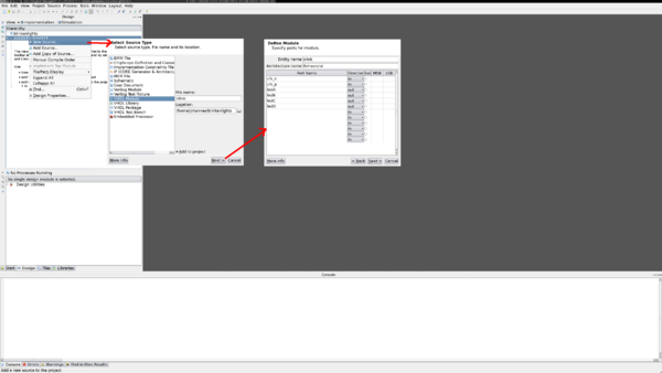
Right click on the xc6slx45-3csg324 folder and create a new file. Select "VHDL Module" and give it a name. In the next window we define the inputs and outputs of the entity. You should define six ports there:
- clk_n: negative pair of the LVDS clock signal (will be explained later)
- clk_p: positive pair of the LVDS clock signal
- ledA: output to control led A on the GPBB
- ledB: output to control led B on the GPBB
- ledC: output to control led C on the GPBB
- ledD: output to control led D on the GPBB
Those signals are only one bit wide so we only need to set the direction and can ignore the MSB/LSB and Bus collumns.
Now ISE should have created an VHDL file for us with the following content:
-- Company:
-- Engineer:
--
-- Create Date:    16:43:49 02/05/2015
 -- Design Name:
-- Module Name:    blink - Behavioral
-- Project Name:
-- Target Devices:
-- Tool versions:
-- Description:
--
-- Dependencies:
--
-- Revision:
-- Revision 0.01 - File Created
-- Additional Comments:
--
----------------------------------------------------------------------------------
library IEEE;
use IEEE.STD_LOGIC_1164.ALL;

-- Uncomment the following library declaration if using
-- arithmetic functions with Signed or Unsigned values
--use IEEE.NUMERIC_STD.ALL;

-- Uncomment the following library declaration if instantiating
-- any Xilinx primitives in this code.
--library UNISIM;
--use UNISIM.VComponents.all;

entity blink is
    Port ( clk_n : in  STD_LOGIC;
           clk_p : in  STD_LOGIC;
           ledA : out  STD_LOGIC;
           ledB : out  STD_LOGIC;
           ledC : out  STD_LOGIC;
           ledD : out  STD_LOGIC);
end blink;

architecture Behavioral of blink is

begin


end Behavioral;
We will need the commented out library declarations so uncomment the use IEEE.NUMERIC_STD.ALL; and library UNISIM; use UNISIM.VComponents.all; lines.
Right now the Code does not do much. To let it do something usefull we need a timesource and thankfully the Novena Board provides one for us but it is a differntial Signal so we need to intepret it and buffer it to be userd in our code to do so we define a signal that we will use as a clock source in the architecture block:
architecture Behavioral of blink is
signal clk: STD_LOGIC;
begin
And feed the two differntial signalsclk_p and clk_n into it. Thankfully there already exists a predefined buffer to do this (in the UNISIM library we just uncommented).
begin
                IBUFGDS_inst : IBUFGDS
                         generic map (
                                 IBUF_LOW_PWR => TRUE,
                                 IOSTANDARD => "DEFAULT"
                        )

                        port map (
                                 O => clk, -- clock buffer output
                                 I => clk_p,       -- diff_p clock buffer input
                                 IB => clk_n      -- diff_n clock buffer input
                        );

end Behavioral;
Now that we have a clk signal we can use it as a time base. But since the clock runs at 50MHz we can't realy see it if we drive an led directly with it. To drive an led we need to subdivide it using a counter that is incremented on each clock cycle. To do this we define an aditional signal in the architecture block signal counter: STD_LOGIC_VECTOR(31 downto 0) :=(others => '0');.
This defines a 32 bit wide signal ((31 downto 0)) filled with 0s at initialisation ( :=(others => '0')) called counter.
To increase the counter on each clock cycle we need to add a process in the architecture block that listens on the clk signal and changes the counter on each rising edge:
        process(clk)
        begin
                if rising_edge(clk) then
                        if counter(31) = '1' then
                                counter <= (others => '0'); -- reset counter if bit 31 is set
                        else
                                counter <= std_logic_vector(unsigned(counter) + 1); -- increase counter if not
                        end if;
                end if;
        end process;
end Behavioral
The std_logic_vector(unsigned(counter) + 1)) conversion is needed since addition is not defined on STD_LOGIC_VECTOR. So we convert the counter to unsigned integer add 1 to it and convert it back to std_logic_vector.
Now we have a signal counter that is increased on each clock cycle. The easiest way to let an led blink with a speed that is slow enough for a human to be visible is to simply take on of the lower bits of the counter. The Novena provides a 50MHz clock so the 26th bit changes every 2^26 / 50Mhz = 0.7s for example.
So to have some leds blink just add an assigment to those leds at the end of the behaviour block (the NOTs are here so that two of the LEDs will turn on even if there is a problem with the clock and the counter stays 0 to help debugging):
		  ledA <= counter(25);
		  ledB <= NOT counter(26);
		  ledC <= counter(27);
		  ledD <= NOT counter(28);
end Behavioral;
The final code should look like this:
----------------------------------------------------------------------------------
-- Company:
-- Engineer:
--
-- Create Date:    16:43:49 02/05/2015
-- Design Name:
-- Module Name:    blink - Behavioral
-- Project Name:
-- Target Devices:
-- Tool versions:
-- Description:
--
-- Dependencies:
--
-- Revision:
-- Revision 0.01 - File Created
-- Additional Comments:
--
----------------------------------------------------------------------------------
library IEEE;
use IEEE.STD_LOGIC_1164.ALL;

-- Uncomment the following library declaration if using
-- arithmetic functions with Signed or Unsigned values
use IEEE.NUMERIC_STD.ALL;

-- Uncomment the following library declaration if instantiating
-- any Xilinx primitives in this code.
library UNISIM;
use UNISIM.VComponents.all;

entity blink is
	Port ( clk_n : in  STD_LOGIC;
	       clk_p : in  STD_LOGIC;
	       ledA : out  STD_LOGIC;
	       ledB : out  STD_LOGIC;
	       ledC : out  STD_LOGIC;
	       ledD : out  STD_LOGIC);
end blink;

architecture Behavioral of blink is
	signal clk: STD_LOGIC;
	signal counter: STD_LOGIC_VECTOR(31 downto 0) :=(others => '0');
begin
	IBUFGDS_inst : IBUFGDS
                generic map (
                                    IBUF_LOW_PWR => TRUE,
                                    IOSTANDARD => "DEFAULT"
                            )

                port map (
                                 O => clk, -- clock buffer output
                                 I => clk_p,       -- diff_p clock buffer input
                                 IB => clk_n      -- diff_n clock buffer input
                         );

	process(clk)
	begin
		if rising_edge(clk) then
			if counter(31) = '1' then
				counter <= (others => '0'); -- reset counter if bit 31 is set
			else
				counter <= std_logic_vector(unsigned(counter) + 1); -- increase counter if not
			end if;
		end if;
	end process;


        ledA <= counter(25);
	ledB <= NOT counter(26);
	ledC <= counter(27);
	ledD <= NOT counter(28);
end Behavioral;
Connecting the Code to the "real world"
Now we have defined the logic for the FPGA and it would run happily on the FPGA but we still need to connect it to the outside world to see some effect. To do this we need to create a "Implementation Constraints File" that describes the connection of the signals in the .vhd file to the real FPGA pins.
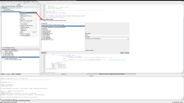
So right click on your .vhd file and select new source and choose "Implementation Constraints File" in the appearing menu.
You should receive an empty file where you define your networks:
#the led pins

NET "ledA" LOC = L1;
NET "ledA" IOSTANDARD = LVCMOS33;
NET "ledA" SLEW = SLOW;

NET "ledB" LOC = L7;
NET "ledB" IOSTANDARD = LVCMOS33;
NET "ledB" SLEW = SLOW;

NET "ledC" LOC = T11;
NET "ledC" IOSTANDARD = LVCMOS33;
NET "ledC" SLEW = SLOW;

NET "ledD" LOC = R11;
NET "ledD" IOSTANDARD = LVCMOS33;
NET "ledD" SLEW = SLOW;

#the differential clock signal is provided at pin H1 and H2
NET "CLK_N" LOC = H1;
NET "CLK_N" IOSTANDARD = LVDS_33;
NET "CLK_N" DIFF_TERM = "TRUE";
NET "CLK_P" LOC = H2;
NET "CLK_P" IOSTANDARD = LVDS_33;
NET "CLK_P" DIFF_TERM = "TRUE";

NET "CLK_P" PERIOD = 20 ns; #the clock runs with 50Mhz (This should tell the compiler to optimize for clock usage and helps the simulator to know which input should be used as clock)
The LOC part defines the pin the network/signal should be attached to. The IOSTANDARD defines which voltage level / transmission standard should be used and the SLEW describes the driving mode (it is set to SLOW here since we don't need any special drivermode).
If you want to use other pins have a look at Novena FPGA Expansion. Or if you want to copy and paste directly look at novena_fpga_tb.v from gpbb-fpga code and novena.ucf from gpbb-fpga code
Generate Programming File
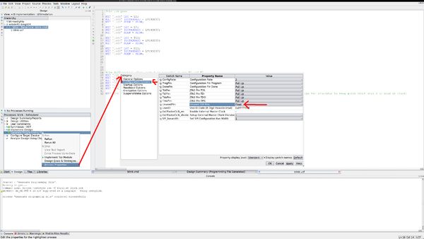
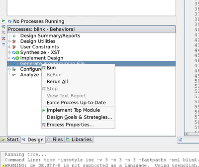
Now you are almost ready to generate the programming file but you have to change some configuration setting first right click on the "Generate Programming File" header and choose "Process Properties" and change "Unused IOB Pins" (under the "Configuration Options" Tab) to "Floating":
The Novena does not seem to like it if all unused pins are pulled down and crashes if you don't change this setting.
Now you can right-click on the "Generate Programming File" header again and choose "Run" this time this should generate a .bit file in your project folder. Transfer this .bit file to your Novena.
Upload to FPGA
To upload the .bit file to the FPGA we use the configure.sh script from the GPBB Example code. To use this code we have to compile the devmem2.c since it is used by configure.sh.
gcc devmem2.c -o devmem2
Then upload your bit file to the FPGA
sudo ./configure.sh blink.bit
After the upload is completed the LEDs should blink "randomly".
Debugging
You can use openocd to debug the FPGA directly.
Download and build openocd with --enable-sysfsgpio. Then, create openocd-novena-fpga.cfg:
#
# Config for accessing the FPGA through the onboard GPIO port.
#

interface sysfsgpio

transport select jtag

# +-------------+--------------+------+-------+---------+
# | Pad name    | Schematic    | GPIO | sysfs | JTAG    |
# +-------------+--------------+------+-------+---------+
# | DISP0_DAT13 | FPGA_RESET_N | 5-07 |  135  | RESET_N |
# | DISP0_DAT14 | FPGA_TCK     | 5-08 |  136  | TCK     |
# | DISP0_DAT15 | FPGA_TDI     | 5-09 |  137  | TDI     |
# | DISP0_DAT16 | FPGA_TDO     | 5-10 |  138  | TDO     |
# | DISP0_DAT17 | FPGA_TMS     | 5-11 |  139  | TMS     |
# +-------------+--------------+------+-------+---------+
# TCK TMS TDI TDO
sysfsgpio_jtag_nums 136 139 137 138
sysfsgpio_srst_num 135

source [find cpld/xilinx-xc6s.cfg]
source [find cpld/jtagspi.cfg]
Run it with:
sudo openocd -f openocd-novena-fpga.cfg
You can then telnet to localhost:4444 or attach gdb to localhost:3333.


